News

These ASU professors have a plan to reuse salty wastewater in Arizona — and save money
January 28, 2026 | KJZZ
With Arizona in drought and cuts likely coming to the state’s allocation of Colorado River water, lots of people are looking for ways to conserve the water we do have.
And that means folks are trying to get creative. Two Arizona State University professors think they’ve figured out a piece of this puzzle.
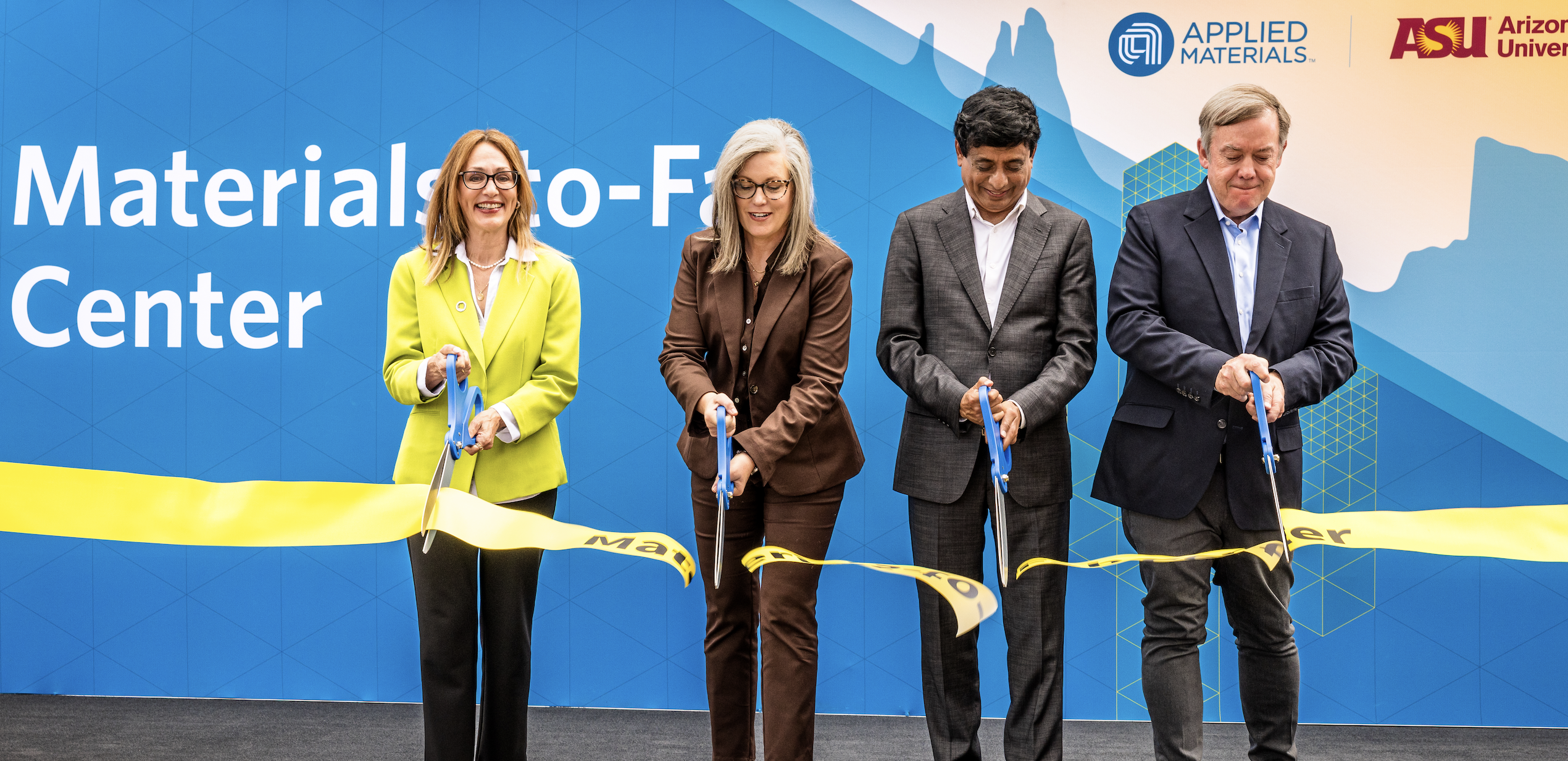
Applied Materials and Arizona State University Celebrate Opening of ‘Materials-to-Fab’ Center
October 9, 2025 | Semiconductor Digest
Applied Materials, Inc. and Arizona State University (ASU) today marked the official opening of the Materials-to-Fab Center, a shared world-class $270 million research, development and prototyping facility inside the university’s MacroTechnology Works at ASU’s Research Park in Tempe. A ribbon-cutting event was held at the Center as semiconductor industry leaders from around the globe gathered in nearby Phoenix for the SEMICON West conference.

ASU faculty member honored with prestigious semiconductor research award
September 16, 2025 | ASU News
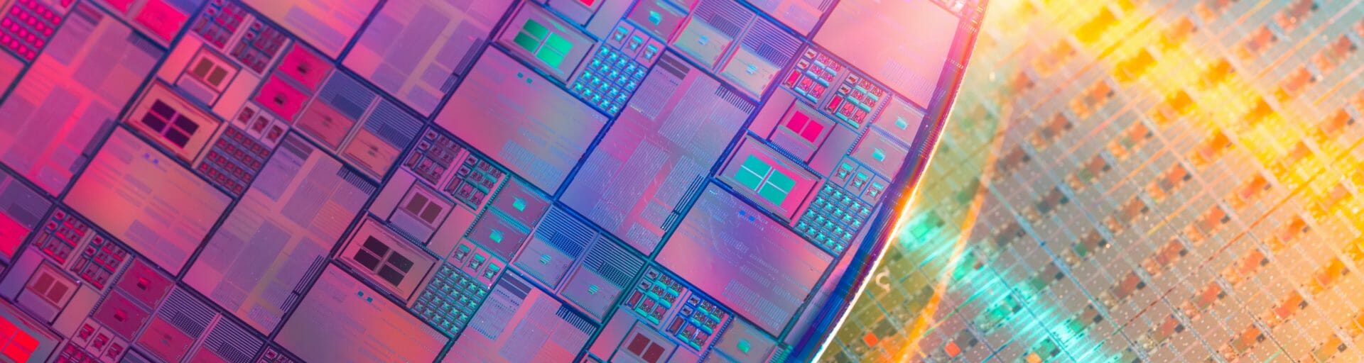
The semiconductor industry is reshaping Arizona’s economic future, driving billions in investments, bolstering workforce development and reshaping the state into a national tech hub.
As this industry’s footprint continues to fortify statewide, one ASU researcher is being recognized for work critical to technologies impacting semiconductor quality and reliability.
More about ASU microelectronics
How the semiconductor boom and ASU are transforming Arizona’s economy
Phoenix’s semiconductor boom is no accident. Years of ASU leadership built the nation’s largest engineering school and cutting-edge facilities driving industry breakthroughs.
Read on news.asu.eduPowering the future of space
ASU researchers pursue innovations in solar space power and propulsion as part of university consortium
Read on fullcircle.asu.eduArizona showcases semiconductor leadership at U.S.-Mexico collaboration forum
To further strengthen economic ties between Arizona and Mexico, Arizona hosted a collaboration forum focused on semiconductor advancement on June 23-24.
Read on azcommerce.comAI-powered smart medicine meets smart microchips
As the largest U.S. supplier of semiconductor equipment, Applied Materials is at the forefront of microchip innovation.
Read on news.asu.eduApplied Materials invests in ASU to advance technology for a brighter future
For nearly 60 years, global giant Applied Materials has been hard at work engineering technology that continues to change how microchips are made.
Read on news.asu.eduArizona attracts “crown jewel” of microelectronics R&D
The state has emerged as the world’s go-to destination for companies charting the future of digital technology.
Read on Sacramento Business Journal