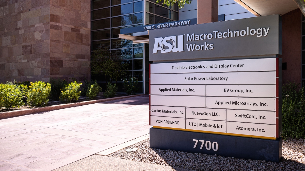
A unique university facility
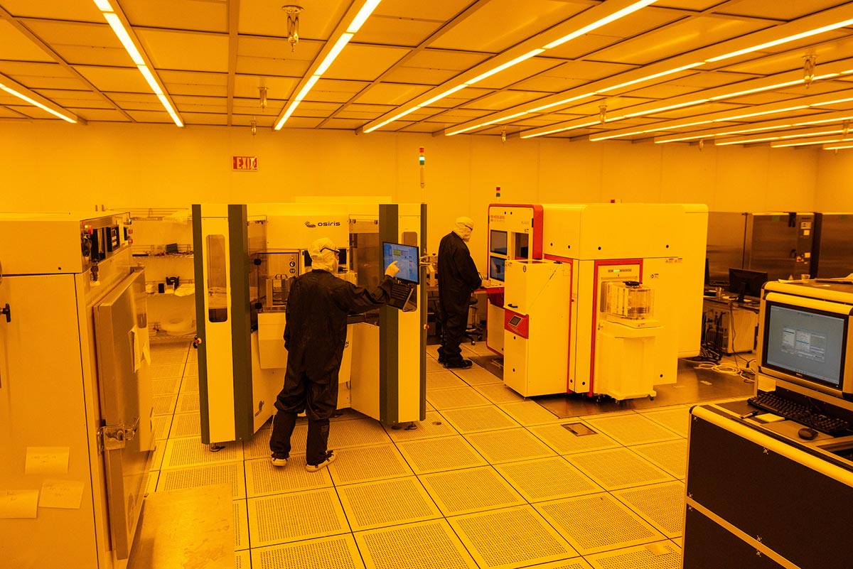
The MacroTechnology Works facility at Arizona State University is a one-of-a-kind asset among U.S. universities. MacroTechnology Works operates as a semiconductor fabrication facility working at industry-standard sizes and specifications, enabling capabilities no other university in the country can offer.
MacroTechnology Works serves as a working lab, fostering collaborations with industry partners in the private sector. From budding startups to established multinational corporations, semiconductor companies are attracted to locate here because ASU’s deep understanding of industry needs enables mutually beneficial collaborations in research, workforce development and education.
This unique facility puts ASU at the forefront of numerous large-scale national research projects and initiatives, including leading projects with:
- Southwest Advanced Prototyping Hub, one of eight regional innovation hubs for the U.S. Department of Defense Microelectronics Commons initiative.
- SHIELD USA, or the National Institute of Standards and Technology Substrate-based Heterogeneous Integration Enabling Leadership Demonstration for the USA, an initiative to advance microelectronics packaging.
- Applied Materials Materials to Fab Center, an innovation partnership with the Silicon Valley-based company that is the leader in materials engineering solutions used to produce virtually every new chip and advanced display in the world.
Collaborative research opportunities
MacroTechnology Works bridges the gap from lab to fab, ensuring innovative technologies reach the market through collaboration among industry partners, government and national defense agencies, and ASU faculty members and students. ASU’s Ira A. Fulton Schools of Engineering offers a comprehensive ecosystem where industry partners can engage with faculty experts on a range of dimensions driving innovation in microelectronics and semiconductor research.
Industry partners lease space within the facility, establishing research agreements with the university to access specialized tools, shared facilities and technical expertise — all with the goal of fostering new opportunities for innovation and business growth. Smaller companies use MTW as a stepping stone to advance their plans, and larger companies use it as an incubator of new ideas and to accelerate their development.
MacroTechnology Works also operates as a foundry for hire, offering flexible models that range from paid equipment access for research and development to building orders to specifications from start to finish. The facility’s industry-standard tools enable full-scale pilot production models, to accelerate the pace of bringing devices to market.
It’s kind of an ecosystem of companies like us that are doing material research in advanced areas. Just being in this environment of innovative companies and talking to people from them in the hallway is helpful.
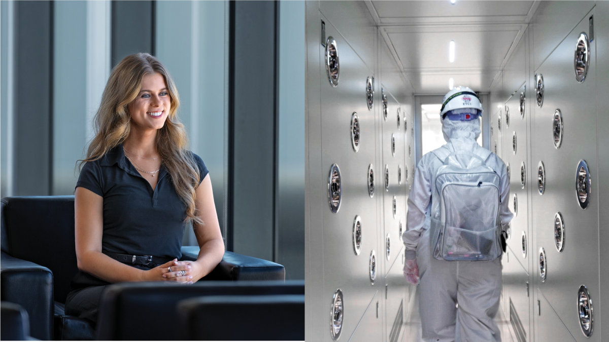
Scott Bibaud, president and CEO of Atomera Atomera, which leases space in MacroTechnology Works, designs a film that helps semiconductor materials move electrons faster.
Advancing the economy in Arizona and beyond
MacroTechnology Works is uniquely designed to play an important role in strengthening U.S. microelectronics manufacturing and positioning Arizona as a national innovation hub. Its infrastructure supports industry growth, providing a home for startups and established companies alike and contributing to the development of talent and the creation of high-paying jobs in the region.
Students gain hands-on research experience in this dynamic environment, preparing them to enter Arizona’s rapidly growing microelectronics sector, where industry leaders such as AMKOR, Intel and TSMC are making investments and expanding operations.
Partner success stories
MacroTechnology Works’ partnerships between ASU and industry have delivered numerous success stories. Among them are:
How the semiconductor boom and ASU are transforming Arizona’s economy
Efforts ASU has led or contributed to have been major factors in the growing economic impact of the semiconductor industry’s growth in Arizona.
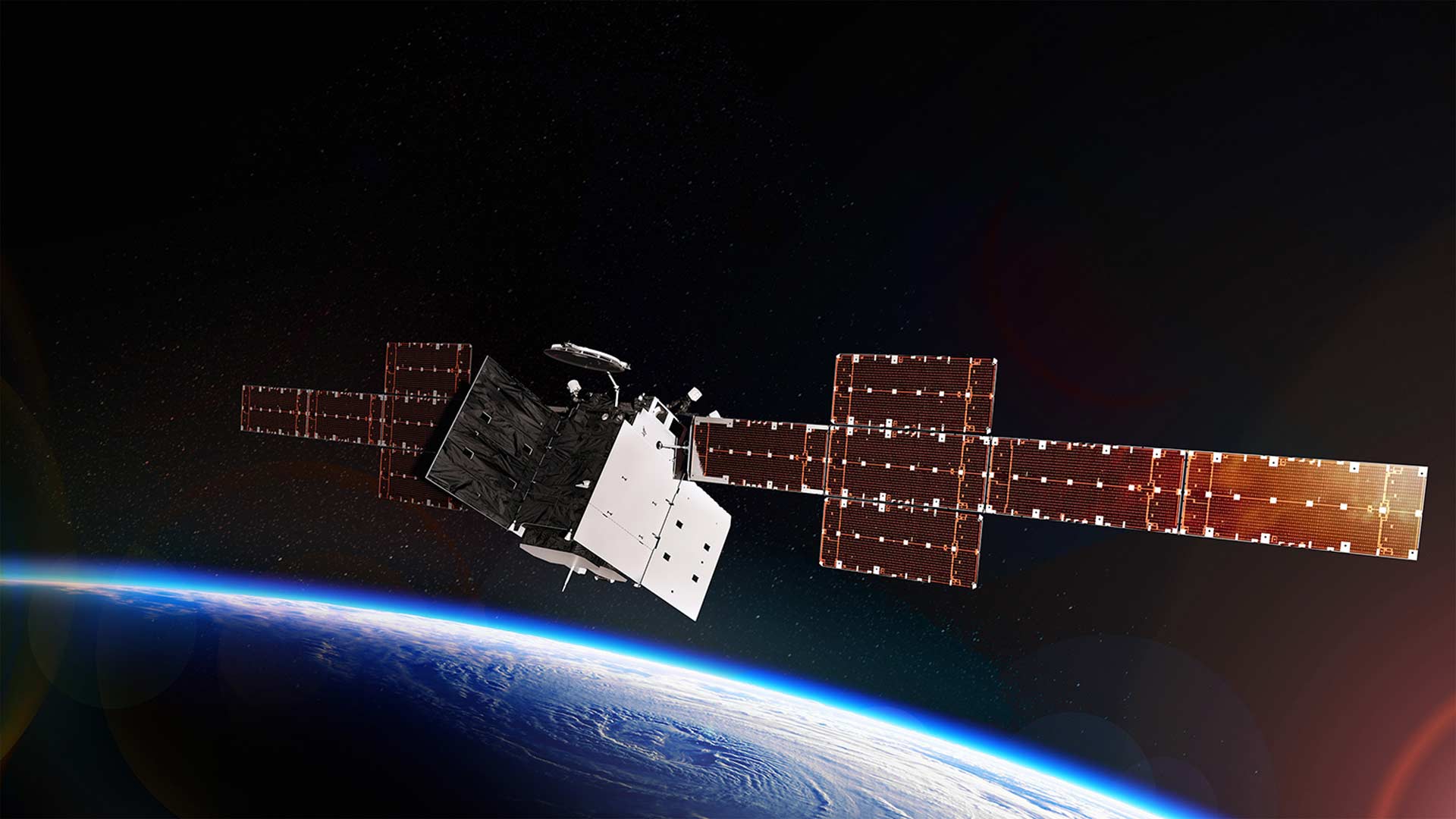
Powering the future of space
As part of a university consortium, researchers in the Fulton Schools are developing innovative solutions for space solar power and propulsion systems.

ASU selected as home and partner for CHIPS and Science Act-funded national facility for semiconductor advanced packaging
ASU Research Park was announced as the site of the co-located NSTC Prototyping and NAPMP Advanced Packaging Piloting Facility.

ASU-led Southwest Advanced Prototyping Hub awarded $21.3M for 2nd year of funding for microelectronics projects
Projects taking place through the SWAP Hub received a second year of funding to advance microelectronics technology for national defense.
ASU and Deca Technologies selected to lead $100M SHIELD USA project to strengthen U.S. semiconductor packaging capabilities
The project will drive innovation and expand capacity in domestic advanced microelectronics packaging and help regain U.S. microelectronics leadership.
Prototyping facility will give students, startups access to semiconductor space
ASU and Applied Materials are collaborating on a $270 million Materials-to-Fab Center, which aims to accelerate the lab-to-fab pipeline.
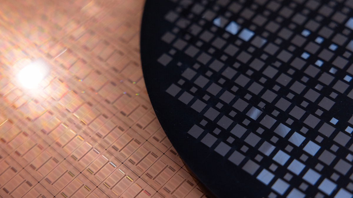
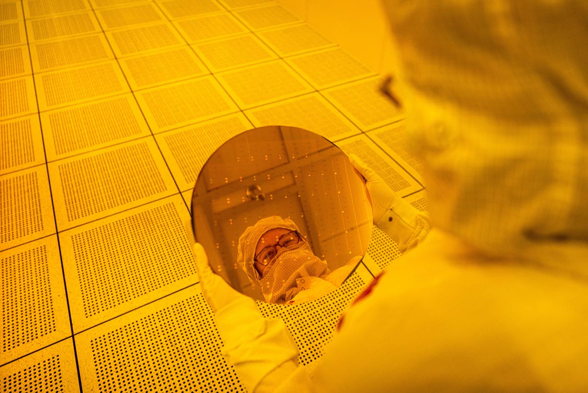
Facilities and capabilities
As a microelectronics prototyping foundry providing production capabilities, MacroTechnology Works houses components of the ASU Core Research Facilities. The Core Facilities provide access to advanced equipment, in-depth consultation and individualized services to achieve research goals on any budget, scale or timeline.
Facilities at MacroTechnology Works include:
- Center for Advanced Wafer-Level Packaging Applications and Development (Coming soon) – Specializing in advanced packaging capabilities for both 200 mm and 300 mm device wafer formats, as well as 300 mm M-Series molded fan-out wafers.
- Advanced Electronics and Photonics – Offering backplane electronics design, fabrication, test and integration capabilities. This facility also operates dedicated pilot line toolsets for technology development and technology demonstrator production.
- Solar Fab – Offering end-to-end solar cell fabrication, characterization and testing capabilities. Additional services include module creation and reliability testing.
Work with us
With all that MacroTechnology Works has to offer industry collaborators, faculty researchers and students, the customizable opportunities to support and work with us are endless.
Connect with us to find out how we can help you achieve your goals.
- Access world-class facilities and infrastructure
- Collaborate with ASU’s experts and researchers
- Tap into America’s most diverse technical talent pool
- Co-locate in Innovation Zones with lab and office space
- Drive next-stage technological breakthroughs