A regional ecosystem for innovation in microelectronics and defense
Led by Arizona State University, the Southwest Advanced Prototyping Hub is one of eight regional innovation hubs established under the Department of Defense’s Microelectronics Commons, a national strategic initiative to accelerate the development and production of microelectronics technologies that are critical to U.S. security and defense. Funded by a $39.8 million initial DoD investment, the SWAP Hub is one of the first awards under the CHIPS and Science Act of 2022, which aims to revitalize American semiconductor manufacturing capacity and competitiveness.
As the SWAP Hub lead, Arizona State University leverages its ability to convene and engage with stakeholders across diverse sectors. The SWAP Hub’s 130+ regional and national partners work together to accelerate the lab-to-fab transition between research, development and production, and collaborate to build the microelectronics workforce of the future through development of curriculum, learning opportunities and job pathways.
ASU coordinates Hub activities and develops the human, physical and digital capabilities of its partners to maximize value to the DoD and advance national security priorities around microelectronics.
130+
SWAP Hub members
6
capability areas
3
cross-cutting themes
comprehensive workforce development
The SWAP Hub brings robust capabilities across all six focus areas of the Microelectronics Commons initiative and develops prototypes for national defense in three priority areas.
Priority areas
Artificial intelligence hardware
5G/6G wireless technology
Commercial leap-ahead technologies
Other capability areas
Electromagnetic warfare
Secure edge computing and the internet of things (IoT)
Quantum technology
Partner with the SWAP Hub
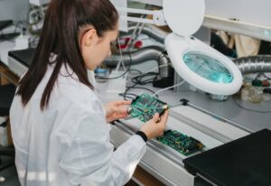
The SWAP Hub’s partners include top semiconductor manufacturers and defense firms, national laboratories, leading academic institutions and numerous organizations and innovative startup companies. Hub partners benefit from access to world-class facilities, advanced equipment and tools, and support from experts at ASU and across the SWAP Hub’s network. The Hub also offers access to calls for proposals on DoD-funded projects and unique opportunities for collaboration.
High fidelity execution and innovation
The SWAP Hub leverages ASU’s sophisticated, mature management systems for working with industry and DoD clients, as well as its extensive experience in managing large-scale federal projects and complex sub-awards. ASU ensures DoD and industry-level rigor in management of SWAP projects through a systems-based manufacturing approach and quality systems model that enables agility and innovation while guaranteeing fidelity and trusted, secure collaboration. Additionally, ASU maintains capabilities to carry out classified work, allowing the Hub to execute projects that require security clearance.

Split-fab innovation for end-to-end success
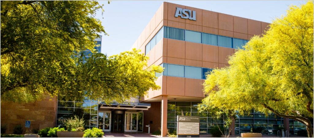
The SWAP Hub leverages a unique “split fab” relationship between Arizona State University and Sandia National Laboratories, enabling a unique synergy of capabilities. Sandia specializes in fabrication of radiation-hardened (Rad-Hard) CMOS wafers with front-end-of-line (FEOL) process steps at its Microsystems Engineering, Science and Applications Complex and Center for Integrated Nanotechnology, and ASU handles back-end-of-line (BEOL) processing customized for CMOS+X at its MacroTechnology Works semiconductor fab.
The SWAP Hub also leverages more than $500 million in investment from the private sector and the State of Arizona, including $270 million from ASU, Applied Materials and the Arizona Commerce Authority for the new Materials-to-Fab Center at ASU’s MacroTechnology Works.
- Macrotechnology Works (MTW) a 250,000 ft2 facility with 43,500 ft2 cleanroom, 22,000 ft2 wet/dry labs with substantial H6 capability
- Materials-to-Fab Center (MTF), a groundbreaking partnership with Applied Materials bringing cutting edge industry tools
- ASU Core Facilities for advanced research, consultation and project execution
- Industry scale operations (300 mm tools up to 370 x 470 mm) to develop, characterize and optimize new materials and processes
- Support offered by ASU’s experienced, professional engineering staff

Sandia key capabilities
- The Microsystems Engineering, Science and Applications (MESA) Complex and the Center for Integrated Nanotechnologies (CINT), two co-joined 200 mm Si (180 nm) and 100 mm III-V capable compound semiconductor fabs
- Co-located R&D and production at largest government-owned microfabrication facility
- Entirely export-controlled, secure and capable of handling classified material
- Low volume, high work mix offers high flexibility and agility
- Capabilities for Heterogeneous Integration
World-class capabilities and expertise
The SWAP Hub applies cutting edge physical and virtual tools and world-class expertise across its workflow—from prototype design to demonstration—leveraging partner capabilities across six capability areas and driving performance across three cross-cutting themes.
Six unique capability areas
Materials for CMOS+X
Rad-Hard CMOS+X Integration
Heterogeneous Integration
Circuits, Architectures, and Test
Metrology and Characterization
Power and RF Electronics
Three cross-cutting themes
Trusted and Assured
The Hub’s project performers are committed to designing, testing, and validating the security and trust of microelectronics from IP design through fabrication, packaging, testing and distribution.
Rad-Hard/Extreme Environment Reliability
Going beyond conventional commercial approaches, the Hub’s projects address potential threats to electronics that operate in space and other extreme radiation environments to guarantee functionality and reliability.
Workforce Development
The Hub produces microelectronics talent tailored to DoD-identified needs through partnership with industry, higher education institutions and non-profit organizations.
Members and partners
Core partners provide capability across all Microelectronics Commons Hubs, including access to at-scale facilities with 300mm Si and 200mm compound capabilities
Capability partners provide capability to the SWAP Hub and its members, including access to hub facilities, equipment, software and expertise; <200mm/Si-based fab capabilities
Siemens Government Technologies
Southern Management Semiconductors & Engineering (SMSE)
Technical University of Munich
Tera Spatial
University of California at Santa Barbara
University of Colorado – Boulder
SWAP Hub executive leadership team

Kyle Squires
Chief Executive Officer, SWAP Hub
Dean, ASU Ira A. Fulton Schools of Engineering
Jason Conrad
Chief Operating Officer, SWAP Hub

Krishendu Chakrabarty
Chief Technology Officer, SWAP Hub
Fulton Professor of Microelectronics, ASU School of Electrical, Computer and Energy Engineering
Benefits of engagement
Access ASU Core Facilities and faculty experts
Capability sharing with 130+ diverse Hub members
Teaming and funding opportunities, including on Microelectronics Commons and other CHIPS Act grants
Workforce development and employee upskilling
Exclusive networking events