ASU infrastructure
World-class R&D facilities
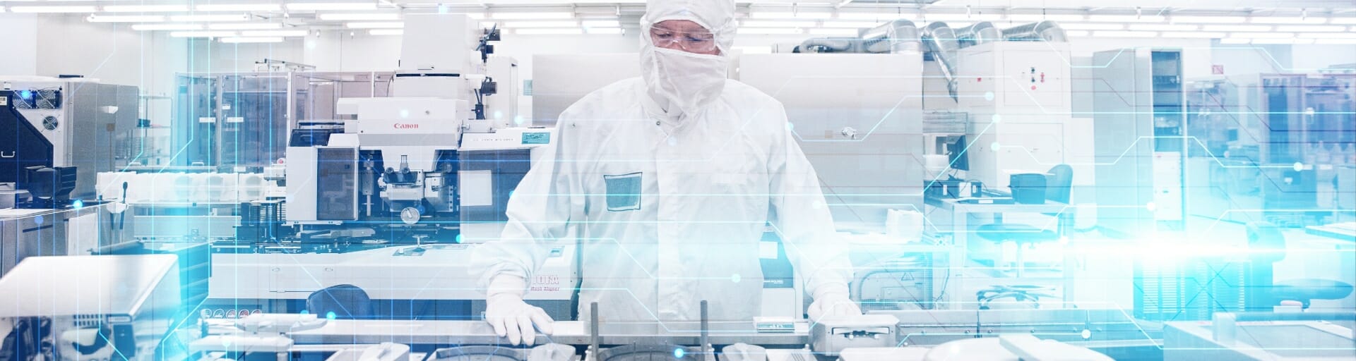
ASU has made significant investments in semiconductor R&D facilities and equipment to ensure the success of industry partners and startups. Through its Core Research Facilities, ASU offers flexible access to state-of-the-art infrastructure, research partnerships with ASU students and faculty, and services and training to solve technical challenges. Users of our Core Research Facilities include local and regional semiconductor enterprises at all scales — from small businesses and startups to multinational firms — as well as other universities and research institutions and government agencies. Through the Microelectronics Industry Council, ASU is rapidly evolving its infrastructure and facilities to anticipate industry needs and stay at the cutting edge of innovation.
Create a customized partnership

Atomera looked all over the world for an institution we could work with to fast-track our advanced semiconductor materials development. We needed a modern, high quality semiconductor fabrication facility combined with leading metrology (measurement and analysis) capabilities. ASU was the facility that provided the best combination of expertise, tool and clean room capabilities, and programs for industry collaboration.
Scott Bibaud President and CEO, Atomera
MacroTechnology Works: a national hub for semiconductor innovation
Located at ASU Research Park, MacroTechnology Works is one of the largest university-based microelectronics R&D facilities in the nation. Originally constructed as a semiconductor fab by Motorola, MacroTechnology Works offers 250,000 square feet of space, including nearly 50,000 square feet of clean room facilities. With flexible wall systems for easy customization of spaces, dedicated wet and dry labs, and sustainable H6-capable space, MacroTechnology Works offers the resources to meet the needs of any partner.
The Materials-to-Fab Center: a new model for university-industry collaboration
ASU and Applied Materials Inc. have teamed up to establish the Materials-to-Fab (MTF) Center, a cutting-edge research, development and prototyping facility co-located with ASU’s MacroTechnology Works.
The MTF Center is a place for collaboration – an environment for not only for ASU and Applied Materials, but also other industry and government partners, startups and academic institutions to fast-track innovation from concept to fab prototype. Equipped with state-of-the-art manufacturing equipment, including 300mm production tools, the MTF Center will enable rapid commercialization of research, accelerate innovation and provide opportunities for hands-on learning that builds the microelectronics workforce.
With investments totaling over $200 million from Applied Materials and an additional $70 million from ASU, the state of Arizona and the Arizona Commerce Authority, the MTF Center represents a strategically innovative approach to strengthening the microelectronics industry in Arizona and across the nation.
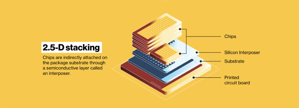
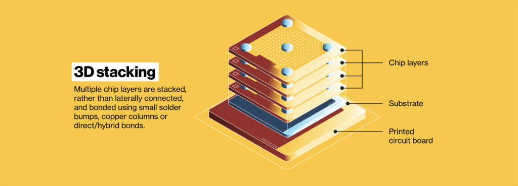
A leading institutional partner for advanced packaging research
Arizona State University is a powerhouse in advanced microelectronics packaging, offering a combination of leading faculty and research staff experts, modern, well-equipped facilities, and valuable supporting resources, including talented and creative students.
These assets make the university a select partner for industry. Companies like Deca Technologies and NXP Semiconductors look to ASU for collaboration and innovation.
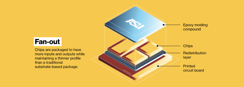
Deca and ASU are working together to create the Center for Advanced Wafer-Level Packaging Applications and Development. The center will advance research in Fan-Out Wafer-Level Packaging (FOWLP) at the 300mm scale used by industry, leveraging the Deca M Series IP to develop advanced packaging technologies. The center will create proven testbeds and novel processes, materials and equipment, bringing innovative technologies from lab to fab, as well as expanding workforce development capabilities.
NXP and ASU are collaborating on FOWLP research as well for design and prototyping solutions for microelectronics to enable emerging technologies, including 6G, internet of things (IoT), machine learning and more. The partnership will also incorporate workforce development capabilities, gallium nitride (GaN) epitaxy research and next-gen GaN device development.
TSMC, Intel and Amkor Technology, which all have Phoenix-area facilities, are also expanding their advanced packaging efforts and will need the advanced packaging workforce ASU is ready to supply.
For these and other partnerships in advanced packaging, the ASU-led Southwest Advanced Prototyping (SWAP) Hub is a valuable asset playing a key role in prototyping abilities including core capability partners in packaging Sandia National Labs and Mercury Systems.

Facilities for collaboration and innovation
Through its Core Research Facilities, ASU provides partners with access to state-of-the-art equipment, services and training to solve their most pressing research challenges. Users of our facilities are diverse, including industry at local, regional, and national scales, as well as government agencies, nonprofits and other universities and research institutions.
Additive Manufacturing Center
Formed as a partnership between ASU, Honeywell Aerospace, Concept Laser (now GE Additive), PADT, Intel and Stratasys, ASU’s Additive Manufacturing Center contains $2 million in state-of-the-art additive manufacturing equipment, including over 20 3D Printers that fabricate parts in polymers, composites and metal, making it the largest additive manufacturing R&D center at any southwestern US university.

Advanced Electronics and Photonics
The Advanced Electronics and Photonics facility provides comprehensive electronics capabilities bridging the high risk, resource-intensive gap between innovation and product development in an information-secure environment. AEP offers backplane electronics design, fabrication, and test and integration capabilities, and operates dedicated pilot line toolsets for technology development.

NanoFab
The NanoFab facility offers state-of-the-art device processing and characterization tools for research and industry partners and specializes in nanofabrication, unique silicon processing, molecular- and bioelectronics, microelectromechanical systems, nano-fluidics, optoelectronics and device characterization.

Solar Fab
The Solar Fab facility offers start-to-finish solar cell fabrication, characterization and testing capability. Additional services include the ability to make modules and to perform fundamental reliability testing.

Eyring Materials Center
The Eyring Materials Center provides researchers with expertise and instrumentation for materials characterization; surface, optical and structural analysis; and high-resolution electron microscopy. It supports materials analysis across a broad range of scientific disciplines, including physics, chemistry, biological sciences, earth and space sciences, and engineering.

Ultrafast Laser Facility
This multi-user facility specializes in time-resolved laser spectroscopy for chemical, biological and material research. It offers advanced laser technologies and instruments for spectroscopic and imaging measurements to observe photophysical and photochemical processes in real time with temporal resolution down to femtosecond time scales and spatial resolution and sensitivity to the point where single molecule signals are detectable.
